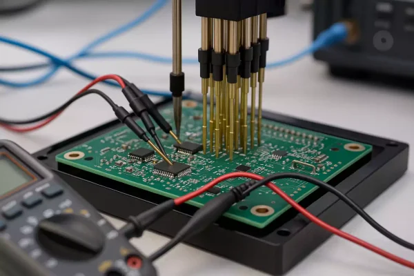
PCB functional testing and inspection in Finland
Optical, X-ray and functional checks layered so that faults are found in Vaasa, not in the field.
In short: Comtec Labs tests assembled circuit boards in Vaasa, Finland. Every board goes through automated optical inspection (AOI), area-array packages such as BGA and QFN are checked with X-ray, and each product then gets the electrical or functional test agreed in its specification. We build test fixtures and test software in-house or run yours, and every result is stored per board or serial number.
Who the testing service is for
Testing is part of every assembly order, but the depth of testing is chosen per product. The service is most valuable for:
- industrial, energy and marine products where a field failure costs far more than a test step
- products with firmware, calibration or communication interfaces that only a functional test can verify
- medical and other regulated products that need records per serial number
- teams that have a test system of their own and want it run on the production floor
How a test strategy is set up
- Test requirements. You tell us what the product must do and what a field failure would cost. If a functional test specification exists, send it with the quote files; if not, we help write it.
- Design for test. Test access is decided in layout, so the DFM review checks test points, a programming and debug connector and how the board is powered on the tester.
- Fixture and software. We design and build the fixture and test software in-house, or integrate the fixture and software you already have.
- Inspection in production. AOI runs on every board straight after soldering, and X-ray checks the hidden joints under area-array packages.
- Electrical or functional test. Each board is programmed where needed and tested to the agreed specification, with the result recorded against its board or serial number.
- Failure analysis and feedback. A failed board is analysed, repaired to IPC-7711/7721 and retested, and the root cause is fed back into the process and, when relevant, into your design.
Test methods compared
No single method finds everything. The table summarises what each common method finds and where it is typically used in the industry.
| Method | What it finds | Typically used for |
|---|---|---|
| AOI | Missing, shifted or reversed parts, bridges and insufficient solder on visible joints | Every board at every volume |
| X-ray | Voids, bridges and opens under BGA, QFN and LGA packages | Area-array packages, class 3 products and first articles |
| Flying probe | Opens, shorts, wrong values and missing parts, without a fixture | Prototypes and runs under about 500 pieces |
| In-circuit test (ICT) | The same faults faster, through a bed-of-nails fixture | Series above about 500 pieces with a stable design |
| Functional test | Whether the product works: power, interfaces, firmware and calibration | The final gate for every product |
By default, Comtec Labs runs AOI on every board, X-ray on area-array packages and the electrical or functional test agreed for the product. For most industrial products, AOI plus a functional test is the sensible minimum.
AOI and X-ray are in-house. Flying-probe and in-circuit testing are arranged through partners on request.
Lead times for test development
AOI and X-ray programmes are prepared as part of the assembly set-up. A functional test takes longer to develop, which is why the test specification is best written before the first prototype. As an industry rule of thumb, a flying-probe programme is generated from CAD data in hours, while an ICT fixture takes 2–4 weeks to build. We confirm the test development schedule with the quote.
Test environment and equipment
Testing takes place in the same ESD-protected production environment in Vaasa as assembly, so boards are not shipped elsewhere between soldering and test. Test fixtures and test software are designed and built in-house, devices can be programmed and provisioned on the production line, and EMC pre-compliance testing is available in-house during development, with formal EMC, safety and radio tests carried out by accredited laboratories.
Functional test benches are built to your test specification and fixtures, and MCUs and FPGAs are programmed on the line.
See the full equipment list, capabilities and lead times
Quality and standards
- Inspection criteria follow IPC-A-610 class 2 as standard and class 3 on request, applied by IPC-trained inspectors.
- Repairs after a failed test are made to IPC-7711/7721 and logged per board with operator and procedure.
- AOI and test results are stored per board, and serial-number traceability is configured per product.
- Root causes are fed back into the process, so the same fault does not repeat in the next batch.
Test instruments are calibrated annually.
What you receive
Test data is only useful if you can read it later. Depending on what we agree for your product, you receive:
- test results per board or per serial number
- first-article inspection reports for new products and revisions
- X-ray images of area-array parts on request
- a yield summary per batch, with the root cause of any failures
When we design the test system for you, the test specification, factory test software and fixture drawings are part of the deliverables, so the test can be reproduced if production ever moves.
Frequently asked questions
Is AOI enough on its own?
For a simple board with no hidden joints and a proven design, AOI plus a functional check can be enough. Any BGA or QFN needs X-ray at least on samples, and any product with firmware needs a functional test.
Can you run our own functional test software?
Yes. We integrate customer test software and fixtures on the production floor, or design and build the complete test system for you.
What happens to a board that fails the test?
It is analysed, repaired to IPC-7711/7721 and retested. The repair is logged against the board, and the root cause is fed back into the process and, if needed, into your design.
When is an ICT fixture worth the cost?
As a rule of thumb in the industry, when annual volume is above roughly 500 boards and the design is stable. Below that, flying-probe or a well-covered functional test is usually more economical.
What should we add to the design to make testing easier?
Give every important net a test point or accessible pad, keep a programming and debug connector, plan how the board is powered on the tester and write the functional test specification before the first prototype.
Related reading
- PCB Testing Methods Explained: AOI, X-ray, Flying Probe, ICT and Functional Test
- Test Points: Small Detail, Big Impact
- What Traceability Should a PCB Assembly Partner Provide? Lot, Serial, Process and Test Records
- The Most Expensive PCB Problems Are Found Too Late
Related services
- PCB assembly
- PCB prototype assembly
- PCB series and low-volume production
- PCB repair and rework
- PCB design services
Request a quote for PCB testing
Send your assembly files together with the test specification, or describe what the product must do. You get the quote and our DFM findings, including test access, usually the same working day and at most within 1 working day.